


1 / 4
$50~1994.49
 0
0![产品详情图片]()
![产品详情图片]()
![产品详情图片]()
![产品详情图片]()
Other Devices · Basic Manufacturing Equipment · Welding Equipment
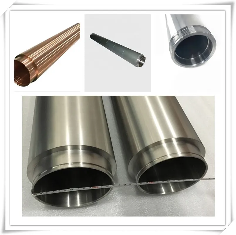
99.95% Metal Niv7 Rotary Tube Nickel Vanadium Alloy Target Material with Polished Surface
Released on2024年09月19 13:23
594 person views
Suppliers
Changsha Xinkang Advanced Materials Co., Ltd.
Attributes
Model NO.XK-NiV
UsagePVD Film Coating
Delivery Time7-21days
KeywordsMetal Nickel Chromium Alloy
PercentNiv7wt%
SizeD50.8X3mm or as Request
Purity99.9%-99.99%
Chemical CompositionNiv7wt%
AppearancePolished Surface
MOQ1PC
Product NameNickel Vanadium Magnetron Sputtering Target
PackageVacuum Blister
Transport PackageVacuum Sealed Package
Specificationcustomized
TrademarkXinKang
OriginHunan, China
Production Capacity1000000 Piece/Pieces Per Month
Product Description
XinKang Top Ranking
Competitive Price Customized Polished Surface 99.95% High Purity NiV7 Nickel Vanadium Alloy Target for PVD Process
Competitive Price Customized Polished Surface 99.95% High Purity NiV7 Nickel Vanadium Alloy Target for PVD Process
Preparation process of nickel-vanadium alloy sputtering target
Material Preparation - Vacuum Induction Melting - Chemical Analysis - Forging - Rolling - Annealing - Metallographic Inspection - Machining - Dimensional Inspection - Cleaning - Final Inspection - Packaging
In the fabrication of integrated circuits, pure gold is generally used as interconnect metal, deposited on a silicon wafer, but gold will diffuse into the silicon wafer to form a high-resistance AuSi compound, which will greatly reduce the current density in the wiring, resulting in the failure of entire wiring system.
So, It is proposed to add adhesive layer between the gold thin film and silicon wafers. The adhesive layer is usually made of pure nickel, but diffusion also occurs between the nickel layer and the gold conductive layer, so that a barrier layer is needed to prevent diffusion between the gold conductive layer and nickel adhesive layer.
With a high melting point and a large current density, vanadium is chosen to deposit barrier layer, therefore, nickel sputtering target, vanadium sputtering target, gold sputtering target are all used in the fabrication of integrated circuits.
Nickel vanadium NiV sputtering targets containing 7% vanadium has both advantages of nickel and vanadium, thus adhesive layer and barrier layer can be achieved at a time. NiV alloy is non-magnetic materials, which is conducive to magnetron sputtering. In the electronics information industry, it is gradually replacing pure nickel sputtering targets.
The picture below are two micrographs of our NiV(93/7 wt%) alloy sputtering target, the average grain size<100μm.
Following is a typically Certificate of analysis for 3N5 NiV 97/3wt% sputtering target.
Application:
Other Related Sputtering Targets
Company Information
FAQ
Loading Product Details
Please wait while we prepare the content...